Spin Defects Under Control
04/06/2021An international research team has made progress towards improved materials for quantum sensor technology. Medicine, navigation and IT could benefit from this in the future.
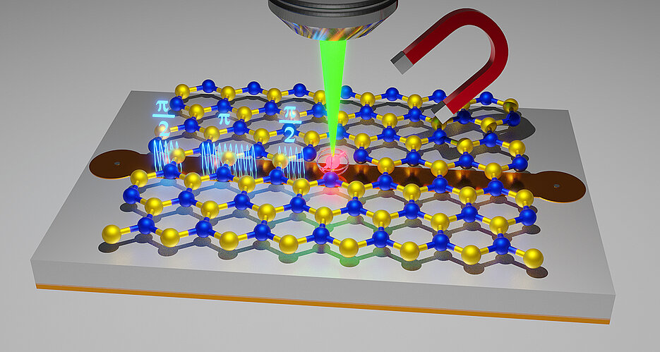
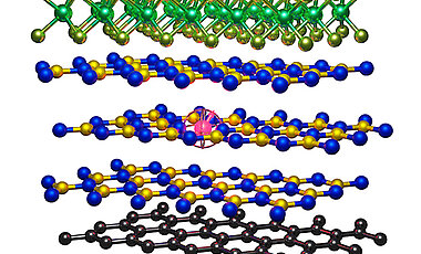
Boron nitride is a technologically interesting material because it is very compatible with other two-dimensional crystalline structures. It therefore opens up pathways to artificial heterostructures or electronic devices built on them with fundamentally new properties.
About a year ago, a team from the Institute of Physics at Julius-Maximilians-Universität (JMU) Würzburg in Bavaria, Germany, succeeded in creating spin defects, also known as qubits, in a layered crystal of boron nitride and identifying them experimentally.
Recently, the team led by Professor Vladimir Dyakonov, his PhD student Andreas Gottscholl and group leader PD Dr. Andreas Sperlich, succeeded in taking an important next step: the coherent control of such spin defects, and that even at room temperature. The researchers report their findings in the impactful journal Science Advances. Despite the pandemic, the work was carried out in an intensive international collaboration with groups from the University of Technology Sydney in Australia and Trent University in Canada.
Measuring local electromagnetic fields even more precisely
"We expect that materials with controllable spin defects will allow more precise measurements of local electromagnetic fields once they are used in a sensor", explains Vladimir Dyakonov, “and this is because they are, by definition, at the border to the surrounding world, which needs to be mapped. Conceivable areas of application are imaging in medicine, navigation, everywhere where contactless measurement of electromagnetic fields is necessary, or in information technology.
"The research community's search for the best material for this is not yet complete, but there are several potential candidates," adds Andreas Sperlich. "We believe we found a new candidate that stands out because of its flat geometry, which offers the best integration possibilities in electronics."
Limits of spin coherence times trickily overcome
All spin-sensitive experiments with the boron nitride were carried out at JMU. "We were able to measure the characteristic spin coherence times, determine their limits and even trickily overcome these limits," says a delighted Andreas Gottscholl, PhD student and first author of the publication. Knowledge of spin coherence times is necessary to estimate the potential of spin defects for quantum applications, and long coherence times are highly desirable as one eventually wants to perform complex manipulations.
Gottscholl explains the principle in simplified terms: "Imagine a gyroscope that rotates around its axis. We have succeeded in proving that such mini gyroscopes exist in a layer of boron nitride. And now we have shown how to control the gyroscope, i.e., for example, to deflect it by any angle without even touching it, and above all, to control this state."
Coherence time reacts sensitively to neighboring atomic layers
The contactless manipulation of the “gyroscope” (the spin state) was achieved through the pulsed high-frequency electromagnetic field, the resonant microwaves. The JMU researchers were also able to determine how long the "gyroscope" maintains its new orientation. Strictly speaking, the deflection angle should be seen here as a simplified illustration of the fact that a qubit can assume many different states, not just 0 and 1 like a bit.
What does this have to do with sensor technology? The direct atomic environment in a crystal influences the manipulated spin state and can greatly shorten its coherence time. "We were able to show how extremely sensitive the coherence reacts to the distance to the nearest atoms and atomic nuclei, to magnetic impurities, to temperature and to magnetic fields - so the environment of the qubit can be deduced from the measurement of the coherence time," explains Andreas Sperlich.
Goal: Electronic devices with spin decorated boron nitride layers
The JMU team's next goal is to realize an artificially stacked two-dimensional crystal made of different materials, including a spin-bearing component. The essential building blocks for the latter are atomically thin boron nitride layers containing optically active defects with an accessible spin state.
"It would be particularly appealing to control the spin defects and their surroundings in the 2D devices not only optically, but via the electric current. This is completely new territory," says Vladimir Dyakonov.
Sponsors of the work
The work was funded by the German Research Foundation DFG and the Alexander von Humboldt Foundation. Vladimir Dyakonov is a Principle Investigator in the Würzburg-Dresden Cluster of Excellence ct.qmat, whose topics include the control of spin-photon interfaces in topological material systems.
Publication
Gottscholl et al., Room Temperature Coherent Control of Spin Defects in hexagonal Boron Nitride, Science Advances 2021, 7, eabf3630, DOI: 10.1126/sciadv.abf3630
Contact person
Prof. Dr. Vladimir Dyakonov, Chair of Experimental Physics VI, University of Würzburg, T +49 931 31-83111, vladimir.dyakonov@uni-wuerzburg.de
Additional images
