Qubits Under Pressure
08/09/2021A new type of atomic sensor made of boron nitride is presented by researchers in "Nature Communications". The sensor is based on a qubit in the crystal lattice and is superior to comparable sensors.
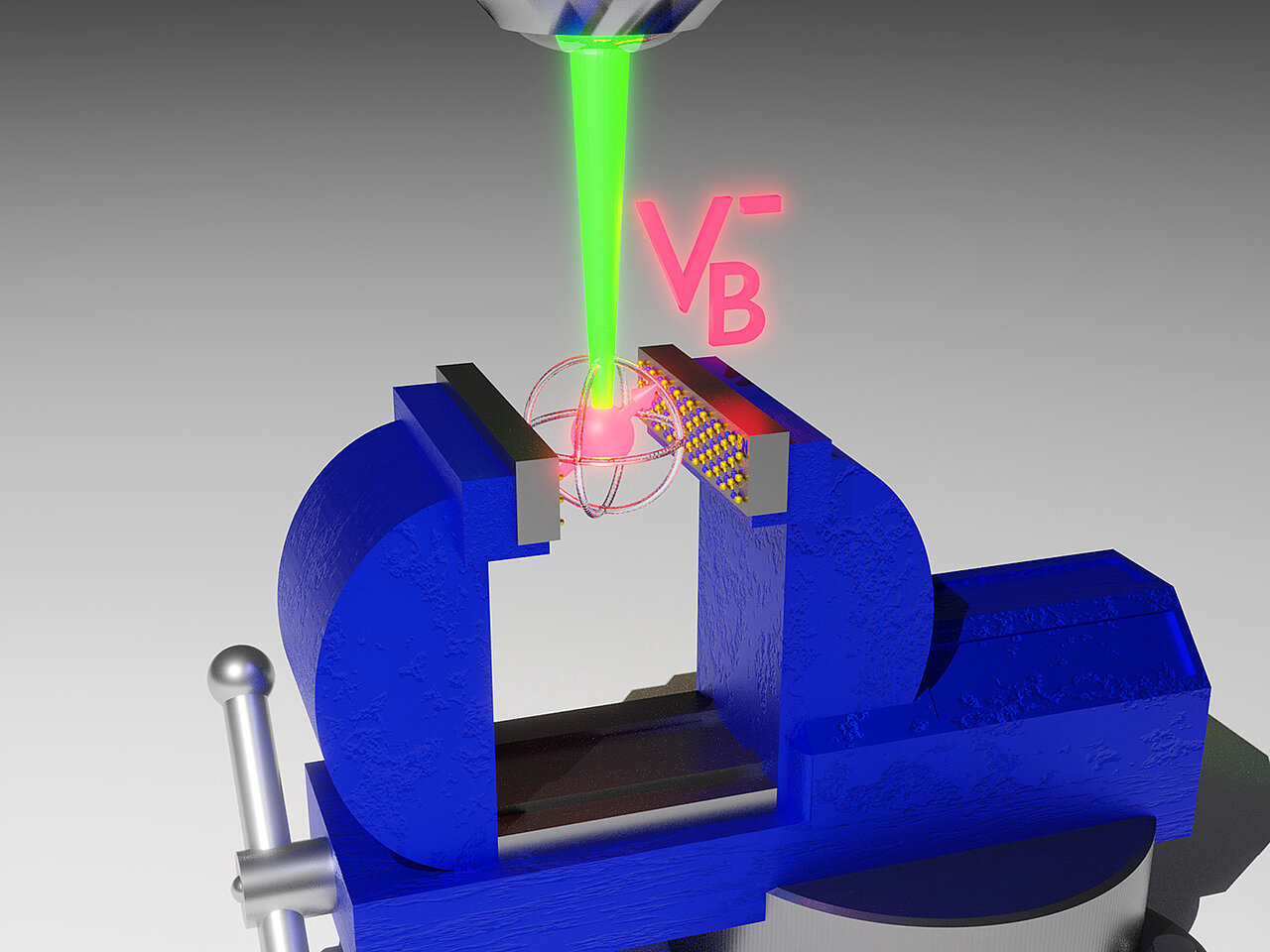
An artificially created spin defect (qubit) in a crystal lattice of boron nitride is suitable as a sensor enabling the measurement of different changes in its local environment. The qubit is a boron vacancy located in a two-dimensional layer of hexagonal boron nitride and has an angular momentum (spin).
The defect is very sensitively to its atomic environment, for example to the distances to other atoms or atomic layers.
"This allows local measurements of magnetic fields, temperature and even pressure," says Professor Vladimir Dyakonov, head of the Chair of Experimental Physics VI at Julius-Maximilians-Universität (JMU) Würzburg in Bavaria, Germany. Measurements are performed completely optically using a laser – therefore, the sensor does not require any electrical contact.
"Modulating microwaves of different frequencies on and off, the spin defect can be manipulated to derive different external influences such as temperature, pressure and magnetic field," explains Andreas Gottscholl. The physics doctoral student at JMU is first author of the publication in the journal Nature Communications, which presents the new sensor.
Characteristics of the novel sensor
Atomic sensors based on spin defects already exist: they are made of diamond or silicon carbide and are suitable for local measurements of temperature and magnetic field. "Our boron nitride sensor provides an additional response to external pressure changes and exceeds the sensitivity of previous systems, especially at low temperatures," explains Gottscholl.
"Another new feature of our spin defect is its location in a two-dimensional crystal lattice. Compared to the established three-dimensional systems based on diamond or silicon carbide, it provides completely new application possibilities," adds the Würzburg physicist.
Example: Boron nitride is currently considered as the standard material for encapsulating of novel 2D devices such as nanometre-sized transistors. "With our work, we have demonstrated that we can artificially embed atomic sensors in the widely used material boron nitride. This should allow to directly measure influences such as temperature, pressure and magnetic field on the investigated devices."
Next research steps
So far, the researchers have demonstrated the functionality of the sensor on a large ensemble of several million spin defects. Next, they want to show sensing with single spin defects. If this succeeds, an application on the nanometre scale would be feasible.
"Particularly interesting is the idea of using boron nitride of only one atomic layer, thus the sensor is positioned directly on the surface of the investigated system," says Professor Dyakonov. This would allow direct interaction with the immediate environment.
Field of application of the sensor
Applications in materials research, device development or biology could be interesting in order to gain new insights in these fields. In addition to other possible scientific implementations, it is also conceivable in the long term to use the spin defect as a commercial sensor– this could revolutionise medical imaging techniques, as the sensor could map local temperatures as an image contrasts, for example.
Cooperations and sponsors
In addition to the team from JMU Physics, Dr. Mehran Kianinia and Professor Igor Aharonovich from the University of Technology Sydney (Australia) as well as Professor Carlo Bradac from Trent University (Canada) are significantly involved in the publication in Nature Communications.
The work was financially supported by the Würzburg-Dresden Cluster of Excellence on Complexity and Topology in Quantum Matter ct.qmat, the Alexander von Humboldt Foundation, the Australian Research Council and the Asian Office of Aerospace Research and Development. JMU supported the publication from its Open Access Publication Fund.
Publication
Spin defects in hBN as promising temperature, pressure and magnetic field quantum sensors, Nature Communications, 22.07.2021, Open Access https://doi.org/10.1038/s41467-021-24725-1
Contact person
Prof. Dr. Vladimir Dyakonov, Chair of Experimental Physics VI, University of Würzburg, Würzburg-Dresden Cluster of Excellence ct.qmat, T +49 931 31-83111, dyakonov@physik.uni-wuerzburg.de