Intern
    Wilhelm Conrad Röntgen Research Center for Complex Material Systems

    TEM (FEI Titan 80-300)

    Transmission Electron Microscope (FEI Titan 80-300)

    Specifications

    • Acceleration voltage: 80 -  300 kV
    • S-Twin objective lens
    • No probe / objective corrector
    • Gatan US1000P camera
    • STEM detector
    • Retractable EDX detector
    • CompuStage low-background double-tilt holder
    • Probe current in 1 nm spot: > 0.6 nA
    • Probe current in 2 nm sport: > 3 nA
    • Maximum spot drift: < 0.5 nm/min
    • Maximum speciment drift: < 0.5 nm/min
    • Resolution (all data for 300 kV)
    • Point resolution: 0.2 nm
    • Line resolution: < 0.1 nm
    • Information limit: < 0.1 nm
    • HAAD-STEM resolution: 0.136 nm - Si (110) dumbells can be resolved
    • Info limit with Lorentz lens: 1.3 nm
    • Point resolution with Lorentz lens: 2.0 nm
    • EDX energy resolution: 133 eV Flexible high tension from 80 to 300 kV

    Location

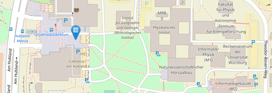
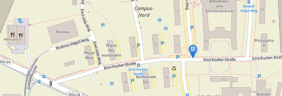
    • Microstructure laboratory

    Pulications

    Comparative Study of the Microstructure of Bi2Se3 Thin Films Grown on Si(111) and InP(111) Substrates
    N. V. Tarakina, S. Schreyeck, T. Borzenko, C. Schumacher, G. Karczewski, K. Brunner, C. Gould, H. Buhmann and L. W. Molenkamp
    Crystal Growth & Design 12, 1913 (2012)

    AlGaInAs quantum dot solar cells: tailoring quantum dots for intermediate band formation
    C. Schneider, S. Kremling, N. V. Tarakina, T. Braun, M. Adams, M. Lermer, S. Reitzenstein, L. Worschech, M. Kamp, S. Hoefling and A. Forchel
    Semiconductor Science and Technology 27, 032002 (2012)

    The Prato reaction on nanodiamond: Surface functionalization by formation of pyrrolidine rings
    D. Langa, A. Krueger
    Diamond and Related Materials 20, 101 (2011)

    Atomically flat single-crystalline gold nanostructures for plasmonic nanocircuitry
    J.-S. Huang, V. Callegari, P. Geisler, C. Brüning, J. Kern, J. C. Prangsma, X. Wu, T. Feichtner, J. Ziegler, P. Weinmann, M. Kamp, A. Forchel, P. Biagioni, U. Sennhauser and B. Hecht
    Nature Communications 1, 150 (2010)

    Atomic scale interface engineering for strain compensated epitaxially grown InAs/AlSb superlattices
    A. Bauer, M. Dallner, A. Herrmann, T. Lehnhardt, M. Kamp, S. Hoefling, L. Worschech and A. Forchel
    Nanotechnology 21, 455603 (2010)